 |
| October 11, 2016 | Volume 12 Issue 38 |
Electrical/Electronic News & Products
Designfax weekly eMagazine

Archives
Partners
Manufacturing Center
Product Spotlight
Modern Applications News
Metalworking Ideas For
Today's Job Shops
Tooling and Production
Strategies for large
metalworking plants
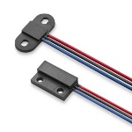
Intro to reed switches, magnets, magnetic fields
 This brief introductory video on the DigiKey site offers tips for engineers designing with reed switches. Dr. Stephen Day, Ph.D. from Coto Technology gives a solid overview on reed switches -- complete with real-world application examples -- and a detailed explanation of how they react to magnetic fields.
View the video.
Bi-color LEDs to light up your designs
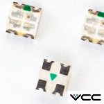 Created with engineers and OEMs in mind, SpectraBright Series SMD RGB and Bi-Color LEDs from Visual Communi-cations Company (VCC) deliver efficiency, design flexibility, and control for devices in a range of industries, including mil-aero, automated guided vehicles, EV charging stations, industrial, telecom, IoT/smart home, and medical. These 50,000-hr bi-color and RGB options save money and space on the HMI, communicating two or three operating modes in a single component.
Learn more.
All about slip rings: How they work and their uses
 Rotary Systems has put together a really nice basic primer on slip rings -- electrical collectors that carry a current from a stationary wire into a rotating device. Common uses are for power, proximity switches, strain gauges, video, and Ethernet signal transmission. This introduction also covers how to specify, assembly types, and interface requirements. Rotary Systems also manufactures rotary unions for fluid applications.
Read the overview.
Seifert thermoelectric coolers from AutomationDirect
 Automation-Direct has added new high-quality and efficient stainless steel Seifert 340 BTU/H thermoelectric coolers with 120-V and 230-V power options. Thermoelectric coolers from Seifert use the Peltier Effect to create a temperature difference between the internal and ambient heat sinks, making internal air cooler while dissipating heat into the external environment. Fans assist the convective heat transfer from the heat sinks, which are optimized for maximum flow.
Learn more.
EMI shielding honeycomb air vent panel design
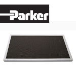 Learn from the engineering experts at Parker how honeycomb air vent panels are used to help cool electronics with airflow while maintaining electromagnetic interference (EMI) shielding. Topics include: design features, cell size and thickness, platings and coatings, and a stacked design called OMNI CELL construction. These vents can be incorporated into enclosures where EMI radiation and susceptibility is a concern or where heat dissipation is necessary. Lots of good info.
Read the Parker blog.
What is 3D-MID? Molded parts with integrated electronics from HARTING
 3D-MID (three-dimensional mechatronic integrated devices) technology combines electronic and mechanical functionalities into a single, 3D component. It replaces the traditional printed circuit board and opens up many new opportunities. It takes injection-molded parts and uses laser-direct structuring to etch areas of conductor structures, which are filled with a copper plating process to create very precise electronic circuits. HARTING, the technology's developer, says it's "Like a PCB, but 3D." Tons of possibilities.
View the video.
Loss-free conversion of 3D/CAD data
 CT CoreTech-nologie has further developed its state-of-the-art CAD converter 3D_Evolution and is now introducing native interfaces for reading Solidedge and writing Nx and Solidworks files. It supports a wide range of formats such as Catia, Nx, Creo, Solidworks, Solidedge, Inventor, Step, and Jt, facilitating smooth interoperability between different systems and collaboration for engineers and designers in development environments with different CAD systems.
Learn more.
Top 5 reasons for solder joint failure
 Solder joint reliability is often a pain point in the design of an electronic system. According to Tyler Ferris at ANSYS, a wide variety of factors affect joint reliability, and any one of them can drastically reduce joint lifetime. Properly identifying and mitigating potential causes during the design and manufacturing process can prevent costly and difficult-to-solve problems later in a product lifecycle.
Read this informative ANSYS blog.
Advanced overtemp detection for EV battery packs
 Littelfuse has introduced TTape, a ground-breaking over-temperature detection platform designed to transform the management of Li-ion battery systems. TTape helps vehicle systems monitor and manage premature cell aging effectively while reducing the risks associated with thermal runaway incidents. This solution is ideally suited for a wide range of applications, including automotive EV/HEVs, commercial vehicles, and energy storage systems.
Learn more.
Benchtop ionizer for hands-free static elimination
 EXAIR's Varistat Benchtop Ionizer is the latest solution for neutralizing static on charged surfaces in industrial settings. Using ionizing technology, the Varistat provides a hands-free solution that requires no compressed air. Easily mounted on benchtops or machines, it is manually adjustable and perfect for processes needing comprehensive coverage such as part assembly, web cleaning, printing, and more.
Learn more.
LED light bars from AutomationDirect
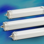 Automation-Direct adds CCEA TRACK-ALPHA-PRO series LED light bars to expand their offering of industrial LED fixtures. Their rugged industrial-grade anodized aluminum construction makes TRACKALPHA-PRO ideal for use with medium to large-size industrial machine tools and for use in wet environments. These 120 VAC-rated, high-power LED lights provide intense, uniform lighting, with up to a 4,600-lumen output (100 lumens per watt). They come with a standard bracket mount that allows for angle adjustments. Optional TACLIP mounts (sold separately) provide for extra sturdy, vibration-resistant installations.
Learn more.
World's first metalens fisheye camera
 2Pi Optics has begun commercial-ization of the first fisheye camera based on the company's proprietary metalens technology -- a breakthrough for electronics design engineers and product managers striving to miniaturize the tiny digital cameras used in advanced driver-assistance systems (ADAS), AR/VR, UAVs, robotics, and other industrial applications. This camera can operate at different wavelengths -- from visible, to near IR, to longer IR -- and is claimed to "outperform conventional refractive, wide-FOV optics in all areas: size, weight, performance, and cost."
Learn more.
Orbex offers two fiber optic rotary joint solutions
 Orbex Group announces its 700 Series of fiber optic rotary joint (FORJ) assemblies, supporting either single or multi-mode operation ideal for high-speed digital transmission over long distances. Wavelengths available are 1,310 or 1,550 nm. Applications include marine cable reels, wind turbines, robotics, and high-def video transmission. Both options feature an outer diameter of 7 mm for installation in tight spaces. Construction includes a stainless steel housing.
Learn more.
Mini tunnel magneto-resistance effect sensors
 Littelfuse has released its highly anticipated 54100 and 54140 mini Tunnel Magneto-Resistance (TMR) effect sensors, offering unmatched sensitivity and power efficiency. The key differentiator is their remarkable sensitivity and 100x improvement in power efficiency compared to Hall Effect sensors. They are well suited for applications in position and limit sensing, RPM measurement, brushless DC motor commutation, and more in various markets including appliances, home and building automation, and the industrial sectors.
Learn more.
Panasonic solar and EV components available from Newark
 Newark has added Panasonic Industry's solar inverters and EV charging system components to their power portfolio. These best-in-class products help designers meet the growing global demand for sustainable and renewable energy mobility systems. Offerings include film capacitors, power inductors, anti-surge thick film chip resistors, graphite thermal interface materials, power relays, capacitors, and wireless modules.
Learn more.
1 nanometer: Lab makes smallest transistor ever
Schematic of a transistor with a molybdenum disulfide channel and 1-nanometer carbon nanotube gate. [Credit: Sujay Desai/UC Berkeley]
For more than a decade, engineers have been eyeing the finish line in the race to shrink the size of components in integrated circuits. They knew that the laws of physics had set a 5-nanometer (nm) threshold on the size of transistor gates among conventional semiconductors, about one-quarter the size of high-end 20-nm-gate transistors now on the market.
But some laws are made to be broken -- or at least challenged.
A research team led by faculty scientist Ali Javey at the Department of Energy's Lawrence Berkeley National Laboratory (Berkeley Lab) has done just that by creating a transistor with a working 1-nm gate. For comparison, a strand of human hair is about 50,000 nm thick.
"We made the smallest transistor reported to date," said Javey, lead principal investigator of the Electronic Materials program in Berkeley Lab's Materials Science Division. "The gate length is considered a defining dimension of the transistor. We demonstrated a 1-nm-gate transistor, showing that with the choice of proper materials, there is a lot more room to shrink our electronics."
The key was to use carbon nanotubes and molybdenum disulfide (MoS2), an engine lubricant commonly sold in auto parts shops. MoS2 is part of a family of materials with immense potential for applications in LEDs, lasers, nanoscale transistors, solar cells, and more.
Berkeley Lab faculty scientist and UC Berkeley professor Ali Javey (left) and graduate student Sujay Desai created the smallest transistor to date. Next to them is a vacuum probe station used to measure the electrical characteristics of the 1-nm-long transistors. [Credit: Marilyn Chung/Berkeley Lab]
The findings were published Oct. 6 in the journal Science. Other investigators on this paper include Jeff Bokor, a faculty senior scientist at Berkeley Lab and a professor at UC Berkeley; Chenming Hu, a professor at UC Berkeley; Moon Kim, a professor at the University of Texas at Dallas; and H.S. Philip Wong, a professor at Stanford University.
The development could be key to keeping alive Intel co-founder Gordon Moore's prediction that the density of transistors on integrated circuits would double every two years, enabling the increased performance of our laptops, mobile phones, televisions, and other electronics.
"The semiconductor industry has long assumed that any gate below 5 nanometers wouldn't work, so anything below that was not even considered," said study lead author Sujay Desai, a graduate student in Javey's lab. "This research shows that sub-5-nanometer gates should not be discounted. Industry has been squeezing every last bit of capability out of silicon. By changing the material from silicon to MoS2, we can make a transistor with a gate that is just 1 nanometer in length, and operate it like a switch."
When electrons are out of control'
Transistors consist of three terminals: a source, a drain, and a gate. Current flows from the source to the drain, and that flow is controlled by the gate, which switches on and off in response to the voltage applied.
Transmission electron microscope image of a cross section of the transistor. It shows the 1-nm carbon nanotube gate and the molybdenum disulfide semiconductor separated by zirconium dioxide, an insulator. [Credit: Qingxiao Wang/UT Dallas]
Both silicon and MoS2 have a crystalline lattice structure, but electrons flowing through silicon are lighter and encounter less resistance compared with MoS2. That is a boon when the gate is 5 nm or longer. But below that length, a quantum mechanical phenomenon called tunneling kicks in, and the gate barrier is no longer able to keep the electrons from barging through from the source to the drain terminals.
"This means we can't turn off the transistors," said Desai. "The electrons are out of control."
Because electrons flowing through MoS2 are heavier, their flow can be controlled with smaller gate lengths. MoS2 can also be scaled down to atomically thin sheets, about 0.65 nm thick, with a lower dielectric constant, a measure reflecting the ability of a material to store energy in an electric field. Both of these properties, in addition to the mass of the electron, help improve the control of the flow of current inside the transistor when the gate length is reduced to 1 nm.
Once they settled on MoS2 as the semiconductor material, it was time to construct the gate. Making a 1-nm structure, it turns out, is no small feat. Conventional lithography techniques don't work well at that scale, so the researchers turned to carbon nanotubes, hollow cylindrical tubes with diameters as small as 1 nm.
They then measured the electrical properties of the devices to show that the MoS2 transistor with the carbon-nanotube gate effectively controlled the flow of electrons.
"This work demonstrated the shortest transistor ever," said Javey, who is also a UC Berkeley professor of electrical engineering and computer sciences. "However, it's a proof of concept. We have not yet packed these transistors onto a chip, and we haven't done this billions of times over. We also have not developed self-aligned fabrication schemes for reducing parasitic resistances in the device. But this work is important to show that we are no longer limited to a 5-nanometer gate for our transistors. Moore's Law can continue a while longer by proper engineering of the semiconductor material and device architecture."
The work at Berkeley Lab was primarily funded by the Department of Energy's Basic Energy Sciences program.
Source: Lawrence Berkeley National Laboratory
Published October 2016
Rate this article
View our terms of use and privacy policy